技術詳情
首頁 > 技術鏈結 > 晶圓疊對量測技術本系統是由高解析工業用相機、顯微物鏡及紅外光源組成紅外疊對顯微模組,採用亮場及背光兩種光源打光,可同時取得晶圓上下兩層高解析單張影像;並藉由後端校正及疊合對位演算法,可自動分析取得高精度之疊對偏差量及疊對圖樣關鍵尺寸結果。
The system is composed of a high-resolution industrial camera, a microscopic objective lens, and an infrared light source, forming an infrared overlay microscopy module. It utilizes both brightfield and backlight illumination to simultaneously capture high-resolution single images of the upper and lower layers of the wafer. Through backend calibration and overlay alignment algorithms, the system can automatically analyze and obtain high-precision overlay deviations and critical dimension results of the overlay patterns.
- CCD可視範圍:800 µm x 600 µm@20x
CCD FOV:800 µm x 600 µm@20x - 最大可量測疊對樣本範圍:100 µm x 100 µm
Maximum Pattern Measuring area:100 µm x 100 µm - 重複性:≤ 0.2 µm (3σ)
Repeatability:≤ 0.2 µm (3σ) - 再現性:≤ 0.4 µm (3σ)
Reproducibility:≤ 0.4 µm (3σ) - 晶圓尺寸:6吋、8吋、12吋
Wafer size:6、8、12 inch wafer
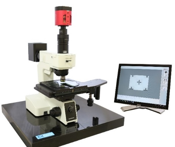
系統外觀圖
- 晶圓疊對偏差量測
Wafer Overlay - 關鍵尺寸量測
Critical Dimension Measurement
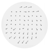
Wafer map
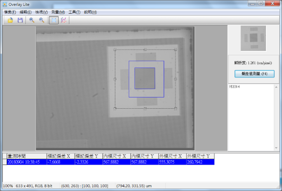
軟體介面圖