技術詳情
首頁 > 技術鏈結 > 晶圓表面形貌量測技術晶圓表面形貌量測系統是利用光偏折原理,由相機擷取晶圓上的條紋影像,並應用相位移及相位展開技術量測條紋變形量,即可測量出晶圓表面斜率變化及表面形貌,並可分析晶圓之翹曲及薄膜應力,本技術可扣除重力影響,重現樣本最真實的翹曲值。
The wafer surface topography measurement system utilizes the principle of light deflection, where a camera captures fringe images on the wafer. By applying phase-shifting and phase-unwrapping techniques to measure fringe deformation, the system can determine surface slope variations and surface topography. It also allows for the analysis of wafer warpage and thin-film stress. This technology can eliminate the effects of gravity, providing the most accurate representation of the sample's true warpage.
- 橫向解析度:220 µm@6” & 8”、300 µm@12“
Lateral resolution:220 µm@6” & 8”、300 µm@12” - 軸向解析度:≤ 1 μm
Vertical resolution: ≤ 1 μm - 翹曲精度:≤ 1 μm
Bow & Warp accuracy:≤ 1 μm - 量測時間:≤ 10 sec/片
Measuring time ≤ 10 sec/wafer - 量測範圍:6吋、8吋、12吋
Measuring area:6、8、12 inch wafer
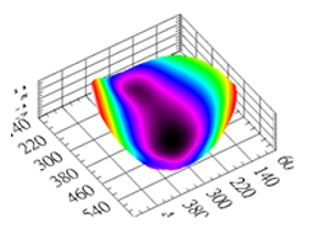
晶圓量測結果
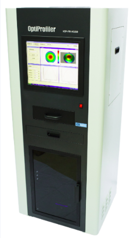
系統外觀圖
- 晶圓翹曲及薄膜應力量測
Wafer warpage/Bow/Film stress - 矽、碳化矽、氮化鎵晶圓
Si, SiC, GaN wafer
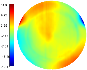
三維高度分布圖
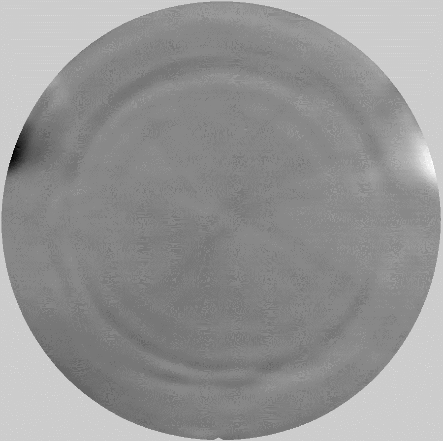
三維紋理圖