技術詳情
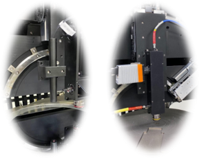
首頁 > 技術鏈結 > 晶圓厚度及薄膜量測技術光譜反射儀是藉由分析光從待測樣品反射之光學特性來獲的待測樣品的相關參數。基本架構為一寬頻光源以一低數值孔徑照明入射至待測樣品,從待測樣品之反射光經由光學系統入射至光譜儀,並轉換為光譜訊號,藉由理論分析及曲線擬合,可獲得待測樣品的相關參數。此量測系統可量測參數為薄膜厚度、晶圓厚度、微結構多參數,像是深度、粗糙度等參數。
A spectroscopic reflectometer analyzes the optical properties of light reflected from a sample to obtain relevant parameters of the sample. The basic setup involves a broadband light source that illuminates the sample with a low numerical aperture. The reflected light from the sample is directed through an optical system into a spectrometer, where it is converted into spectral signals. Through theoretical analysis and curve fitting, the relevant parameters of the sample can be determined. This measurement system can measure parameters such as thin film thickness, wafer thickness, and various microstructure parameters, including depth and roughness.
- 薄膜厚度範圍:100 nm – 150 µm
Thickness range:100 nm – 150 µm - 薄膜厚度量測重覆性:≤ 1.0 nm
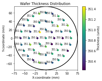
Thickness repeatability:≤ 1.0 nm - 晶圓厚度量測範圍:10 µm – 500 µm
Wafer thickness repeatability:10 µm – 500 µm - 晶圓厚度量測重覆性:≤ 0.5 µm
Wafer thickness repeatability:≤ 0.5 µm - 量測點大小:2 mm 或 50 µm
Spot size:2 mm (macro-type) or 50 µm (micro-type) - 量測範圍:6吋、8吋、12吋
Measuring area:6、8、12 inch wafer
- 薄膜厚度量測
Thin film measurement - 晶圓厚度量測
Wafer thickness measurement - 矽、碳化矽、氮化鎵晶圓
Si, SiC, GaN wafer