技術詳情
首頁 > 技術鏈結 > 晶圓表面形貌及粗糙度量測技術白光干涉儀量測模組採用低相干干涉原理,利用寬頻白光源照射樣品,並透過干涉條紋的相位與強度分析,獲得奈米級的三維表面形貌與高度資訊。本技術具備非接觸、高精度與快速量測等特性,特別適用於半導體晶圓表面形貌及粗糙度等參數量測。
The white light interferometer module uses low-coherence interferometry, where a broadband light source illuminates the sample and interference fringe phase and intensity are analyzed to obtain nanometer-level 3D surface profiles and height information. Featuring non-contact, high-precision, and fast measurement, it is ideal for wafer topography, and roughness measurement。
- 晶圓表面形貌量測範圍:1 μm – 400 μm
Topography height range:1 μm – 400 μm - 晶圓表面形貌量測重覆性:≤ 0.1 μm
Topography measurement repeatability:≤ 0.1 μm
側向量測解析度:≥ 0.1 μm
Lateral resolution:≥ 0.1 μm
縱向量測解析度 ≥ 1 nm
Vertical resolution:≥ 1 nm - 晶圓表面粗糙度量測範圍:≥ 1.0 nm
Roughness measurement range:≥ 1.0 nm - 晶圓表面粗糙度量測重覆性:≤ 0.1 nm
Roughness measurement repeatability:≤ 0.1 nm - 量測範圍:6吋、8吋、12吋
Measuring area:6、8、12 inch wafer
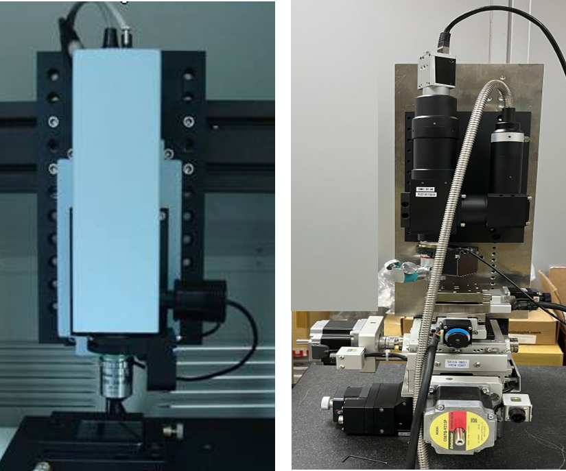
系統外觀圖
- 晶圓表面形貌量測
Wafer Surface Topography measurement - 晶圓表面粗糙度量測
Wafer Surface Roughness measurement - 矽、碳化矽、氮化鎵晶圓
Si, SiC, GaN wafer
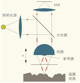
晶圓表面粗糙度量測技術
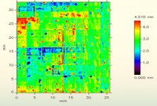
晶圓表面粗糙度分析圖