技術詳情
首頁 > 技術鏈結 > 原子力顯微鏡量測技術AFM為半導體與奈米材料分析用量測系統,可量測參數為三維表面形貌、表面粗糙度(Ra/Rq)、階高(Step height)及奈米級尺寸等。以奈米級探針搭配微懸臂樑掃描樣品表面,量測探針尖端與樣品表面原子間交互作用力所產生的微小偏折,並透過回饋演算建構出樣品的高解析度三維形貌及物理特性。
AFM system can measure the parameters of 3D surface topography, surface roughness(Ra/Rq), step height, and nanoscale dimensions. The nanoscale surface measurement system adapts a nanoscale probe and a microcantilever to measure the minute deflection caused by the atomic interaction force between the probe tip and the sample surface. The high-resolution 3D topography and physical properties of the sample could be calculated and constructed by the feedback system and algorithm.
- Minimum Feature Size Resolved, Z: ~0.1 nm
- Minimum Feature Size Resolved, X & Y: ~2 nm
- X & Y scan range: 90 μm x 90 μm
- Z scan range: up to 10 μm
- Z noise floor: <30 pm RMS
- Sample Size: ≤210 mm diameter, ≤15 mm thick
- Motorized position stage (X-Y axis): 180 mm × 150 mm inspectable area; 2 μm repeatability, unidirectional; 3 μm repeatability, bidirectional
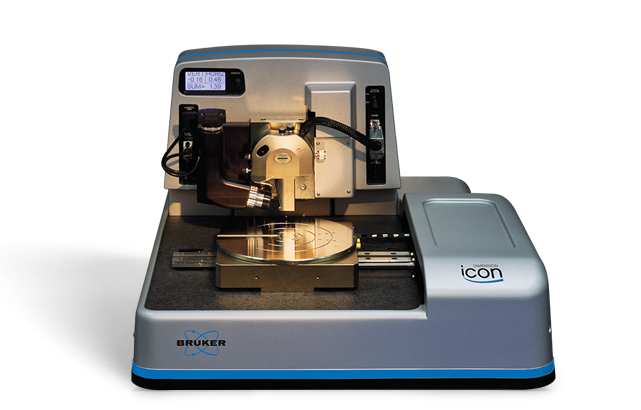
AFM Measurement system
- 三維表面形貌量測
Topography measurement - 表面粗糙度量測
Surface roughness measurement - 相位影像與材料相識別
Phase imaging and material identification - 微區電性量測
Local electrical property measurement
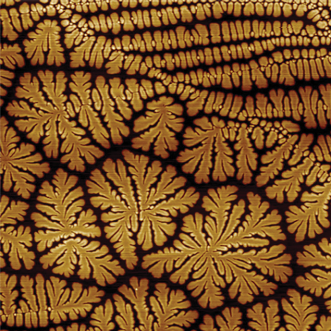
Tapping mode
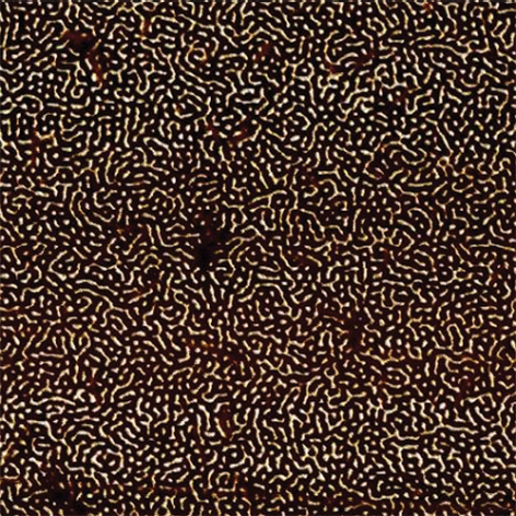
Phase Imaging Mode
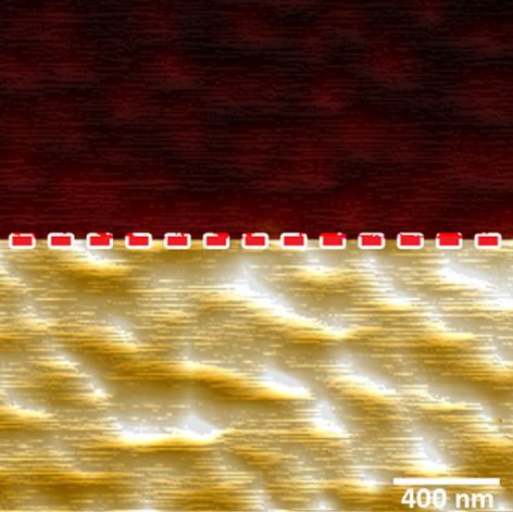
Electric Force Microscopy