技術詳情
首頁 > 技術鏈結 > 掃描式電子顯微鏡量測系統掃描式電子顯微鏡運用電子槍發射高能量之電子束,並以磁力透鏡、電場透鏡聚焦於樣品表面,使其激發出各式訊號,藉此獲得形貌、原子組成、晶格結構、尺寸等訊息。
A scanning electron microscope (SEM) uses an electron gun to generate a high-energy electron beam, which is focused onto the sample surface by electromagnetic lenses. The interaction between the incident electron beam and the sample generates various signals, enabling the characterization of surface morphology, elemental composition, crystal lattice structure, dimensions, and other material properties.
- Sample size: Up to 8-inch wafers
- Tip current: 4 pA ~ 10 nA
- Maximum resolution: 1.0 nm @ 15kV, 1.7 nm @ 1 kV
- Working distance: 8.5 mm
- Magnification: 12x ~ 900000x
- Electron source: Thermal field emission
- Accelerating voltage: 0.1 kV ~ 30 kV
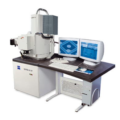
Scanning Electron Microscopy
- 線距量測
Pitch measurement - 奈米粒子粒徑量測
Nanoparticle size measurement - 表面形貌分析
Surface morphology analysis
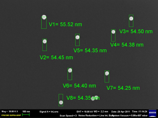
Pitch and Nanoparticle size measurement