技術詳情
首頁 > 技術鏈結 > 晶圓表面粒子檢測技術以雷射掃描檢測晶圓表面,若有粒子或缺陷在晶圓表面,就會產生散射光,散射的光強度與粒子大小有正相關,校正後即可檢測晶圓上所有粒子的尺寸與數量。本技術採用自主設計之傾斜入射投、收光雷射散射模組與晶圓承載機構,適用於檢測透明晶圓及載板,可取代國外設備,並增加應用範圍。
Laser scanning is used to inspect the surface of a wafer. If particles or defects are present on the wafer surface, they will generate scattered light. The intensity of the scattered light is positively correlated with the particle size. After calibration, the size and number of all particles on the wafer can be detected. This technology employs a self-designed tilted incident laser scattering module and wafer carrier mechanism, suitable for inspecting transparent wafers and substrates. It can replace foreign equipment and expand its application range.
- 檢測最小粒徑:0.2 μm
Minimum particle size detected: 0.2 μm - 檢測速度:< 3 分鐘 @ 6吋晶圓
Detection speed: < 3 minutes @ 6-inch wafer - 最大可檢測晶圓:12吋
Maximum inspectable wafer size: 12 inches - 適用晶圓材質:Si / SiC / Glass
Applicable wafer materials: Si / SiC / Glass
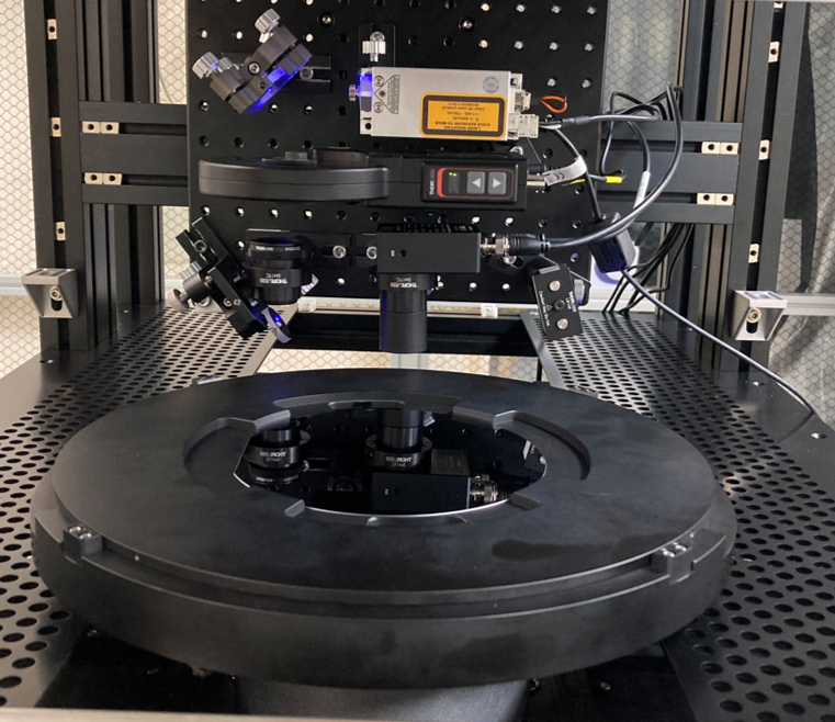
檢測模組 inspection module
- 裸晶圓表面汙染/缺陷檢測與分析
Detection and analysis of surface contamination/defects on bare wafer
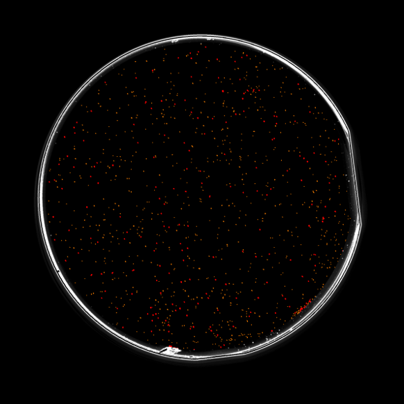
檢測結果 inspection result