技術詳情
首頁 > 技術鏈結 > FOUP式EUV劑量量測儀EUV微影為5 nm以下先進製程的關鍵技術。曝光劑量、均勻性及機台間匹配,須以具明確定義與計量追溯的量值確認。現行半導體微影製程通常需經一系列製程程序,才能回推輻射劑量與機台設定之關係。
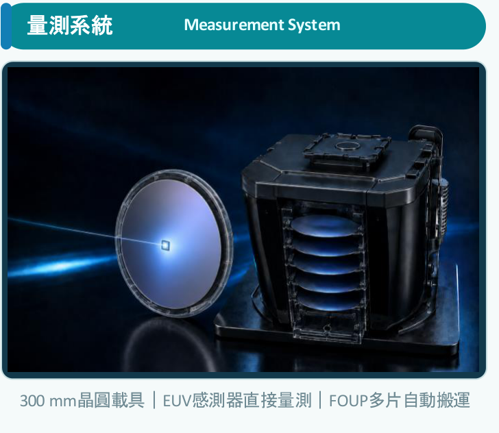
導入可追溯標準件與即時量測技術後,可直接量測曝光位置的輻射劑量(radiant exposure,單位:mJ/cm²),將流程縮短至數分鐘,並於不中斷產線下取得即時資訊。結合FOUP式多片晶圓型EUV感測器與AMHS,可實現自動載運、量測與校正;適用於晶圓廠、EUV光學元件、光阻、材料、設備及檢測業者。
EUV lithography is a critical technology for advanced semiconductor manufacturing processes below 5 nm. Exposure dose, uniformity, and tool matching must be confirmed using clearly defined and traceable measurement quantities. Current lithography processes typically require multiple subsequent processing steps to correlate radiation dose with tool settings.
By introducing traceable standards and real-time metrology, the radiant exposure (in mJ/cm²) at the exposure position can be directly measured, reducing the evaluation cycle to minutes without interrupting the production line. Integrated with a multi-wafer FOUP-type EUV sensor system and AMHS, automated transport, measurement, and calibration are enabled. Applicable to wafer fabs, EUV optical components, photoresists, materials, equipment, and metrology suppliers.
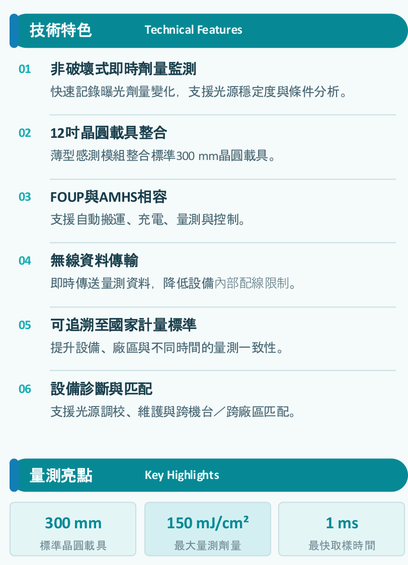
- 適用載具:12吋(300 mm)晶圓載具
- 量測項目:EUV輻射劑量、曝光穩定度與劑量變化
- 最大量測劑量:150 mJ/cm²
- 最快取樣時間:1 ms
- 資料傳輸:無線傳輸
- 系統整合:FOUP控制站/AMHS相容
- 標準追溯:可溯源至國家計量標準
- 應用情境:調校、維護、驗證及跨機台/跨廠區匹配
- EUV光源調校 (EUV source tuning)
- 設備維護 (Equipment maintenance)
- 製程驗證 (Process verification)
- 跨機台/跨廠區匹配 (Tool & fab matching)