技術詳情
首頁 > 技術鏈結 > 光譜式反射儀量測技術FilmChek為光電半導體用量測系統,可量測參數為薄膜厚度(d)、材料折射率(n)、消散係數(k)及矽晶圓矽通孔深度等。以光譜儀搭配取像探頭,量測一寬頻光源入射薄膜及基板後的反射干涉光譜,並透過演算法計算出薄膜材料的厚度、折射率及消光係數。
FilmChek system can measure the parameters of film thickness(d), refractive index(n), extinction coefficient (k), and silicon wafer TSV(through silicon via) depth. The thin film properties measurement system adapts a spectrometer and an image sensor head to measure the reflective interference spectrum of the broadband light source which incident into thin film and substrate. The thickness ,refractive index, and extinction coefficient of the thin film could be calculated by the algorithm.
- Spot size: φ40 μm (5X)
- Wafer size: 4”, 6”, 8”, 12” (glass carrier compatible)
- Film thickness range: 500 Å ~ 30 μm (option to 800 μm )
- Repeatability: < 10 Å @ 5000 Å Oxide on Si substrate
- Automatic stage: r - θ
- Oxide, Nitride, PR, PI film on Si, GaAs, glass, wafer, TSV depth
- Excellent for patterned film with auto mapping
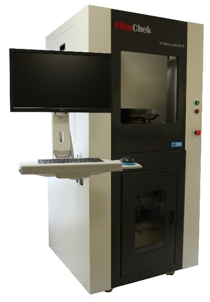
FilmChek Measurement system
- 薄膜厚度量測
Thin film thickness measurement - 厚膜厚度量測
Thick film thickness measurement - 矽通孔深度量測
TSV depth measurement - 折射率及消散係數量測
n & k optical parameters measurement
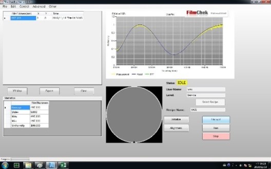
Graphic user interface
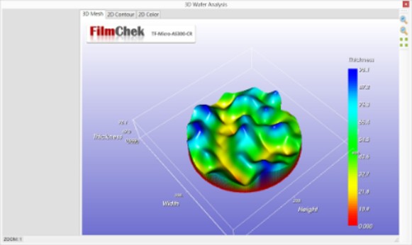
Thin film thickness mesh